Project description:
The rapid development of all modern technologies is largely based on the advancement and availability of electronic components that enable the functioning of most things familiar to us — from a TV remote to artificial intelligence. For many years, the cutting edge of technology has been associated with achieving the smallest possible dimensions of semiconductor structures. In particular, processors based on 2 nm technology are already a reality. However, this also means that further technological progress through miniaturization is becoming impossible, creating the need to search for alternative materials and concepts.
Moreover, there is a vast number of applications that either do not require such critically small dimensions — such as various types of sensors — or cannot be implemented in nanometer-scale devices due to fundamental physical limitations. In particular, optoelectronic technologies, especially in the infrared and terahertz ranges, are only possible with components comparable in size to the wavelength of the corresponding range — that is, from submicrometer to tens of micrometers. Therefore, an active search for new materials or new ways to utilize them more effectively continues relentlessly in the field of micron-scale technologies.
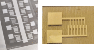
This project aims to establish the infrastructure required for the use of maskless photolithography (MPL), which would enable the development of micro- and optoelectronic devices of a wide range of architectures and applications. MPL technology allows the formation of functional elements of arbitrary shapes, similar to a laser engraver — by “drawing” with an optical (laser) beam on a photoresist film or an active element. The shape and dimensions of the components can be easily modified in the software settings, which significantly accelerates the development process of a specific microelectronic device, as it eliminates the need to manufacture a photomask each time — a complex and costly technology that is practically unavailable in Ukraine.
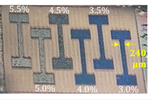
At the first (reporting) stage of the project, a study was carried out to investigate the possibility of controlled modification of the properties of different types of materials using commercial laser engravers. This was a preparatory stage intended to identify the most promising materials and irradiation regimes (wavelength, power, pulsed or continuous operation). Based on the collected data, the next stages of the project will focus on refining the technology of high-resolution maskless photolithography using a modern photolithography system planned for purchase next year.